
Another Wavelength: Cory Boone
This month on Another Wavelength, we meet Tucson native and senior Cory Boone, who began his academic career at the University of Arizona in the mechanical engineering program.
What brought you to study optics?
I started at the University of Arizona studying mechanical engineering. Freshman year I took a tour of the optics building and was blown away by the demos I saw, the art and optical devices around the building and the architecture of the building itself. After this I did lots of research about optical engineering, switched my major as soon as possible, and never looked back.

Who is your hero in science?
My hero in science is Max Plank, who a Nobel Prize in Physics for his work on quantum theory. Plank demonstrated the quantized nature of light, completely changing the field of optics. In my sophomore year of high school I saw a television program explaining quantum mechanics in the simplest terms possible, and it was at that moment that I decided I wanted to be a physicist or engineer. Plank was also very musically gifted and played several instruments. I am a musician myself and I think that music and math go very well together. Maybe I'll have a scientific constant named after me one day and students will be forced to memorize the Boone constant.
Describe your research in 20 words or fewer.
Characterizing the composition and microstructure of materials using scanning electron microscopy, atomic force microscopy, and energy dispersive spectroscopy.
Describe your research in 200 words or fewer.
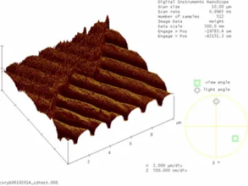
I currently am not involved in much research on campus as I am working at Edmund Optics designing a line of laser-focusing lenses, but in the past I worked with Dr. Tom D. Milster. I still am the safety coordinator for the research group, but last year I had several jobs including characterizing the composition and microstructure of materials using scanning electron microscopy, atomic force microscopy and energy dispersive spectroscopy. For example, I used atomic force microscopy to quantify the pitch, duty cycle and groove depth of gratings. An atomic force microscope scans an extremely small and sharp tip across the surface of a sample. A very accurate topological map of the sample is generated using the deflection of tip due to atomic repulsion by the sample.
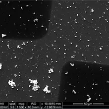
A scanning electron microscope uses a concentrated beam of electrons to image a conductive sample, and an energy dispersive spectrometer is an attachment to an SEM that can determine a material's atomic composition. We were making silver checkerboard patterns on silicon substrates but we always seemed to have some kind of contamination on our samples (picture attached). I used energy dispersive spectroscopy to figure out the composition of the pesky contamination. It turns out that it was actually flakes of silver left over from our deposition process, and we were able to improve this by tweaking that process. I really like this kind of metrology and I'm very thankful that I had the chance to get to learn these techniques at the university.
Name three neat facts about you.
- I've evacuated a burning airplane ... with my 80-year-old grandma.
- When I took the PSAT in high school, I realized that I didn't know how to spell my middle name. I guessed and thankfully got it right.
- I went on tour in China for a month playing drums with the UA jazz band. Many people there had never seen red hair before. I was an alien.